
搜索结果: 1-8 共查到“国际动态 电子科学与技术 the materials”相关记录8条 . 查询时间(0.078 秒)
复旦大学材料科学系方晓生课题组在Nature Reviews Materials期刊发表低维宽禁带半导体用于紫外光探测器的研究综述(图)
方晓生 低维宽禁带 半导体 紫外光探测器
2023/11/21
精确的紫外光检测是现代光电技术的重要组成部分,现阶段的紫外光探测器主要基于宽禁带半导体,例如,III-V半导体。然而,传统的宽禁带半导体在实际应用中达到了瓶颈,难以兼顾高集成度和高柔性。有鉴于此,低维宽禁带半导体由于具有合适的紫外光吸收范围、可调节的光电性能以及良好的衬底兼容性等优势,在多种紫外光工作场景中展现出巨大的应用潜力。

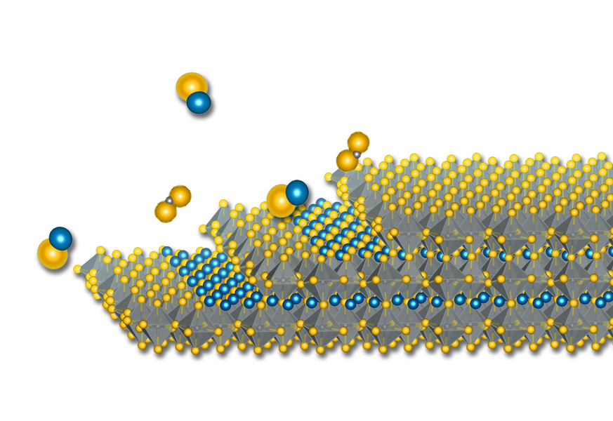
MIT engineers grow “perfect” atom-thin materials on industrial silicon wafers(图)
工业硅晶圆 原子薄材料 芯片
2023/6/6
True to Moore’s Law, the number of transistors on a microchip has doubled every year since the 1960s. But this trajectory is predicted to soon plateau because silicon ― the backbone of modern transist...
Engineers report a major advance in creating a new family of semiconductor materials(图)
半导体材料 硫族化 物钙钛矿 太阳能电池
2023/6/7
MIT engineers report creating the first high-quality thin films of a new family of semiconductor materials. The feat, which lead researcher Rafael Jaramillo refers to as his “white whale” because of h...

New ultrathin semiconductor materials exceed some of silicon’s ‘secret’ powers,Stanford engineers find(图)
New ultrathin semiconductor materials silicon secret powers Stanford engineers
2017/9/5
The next generation of feature-filled and energy-efficient electronics will require computer chips just a few atoms thick. For all its positive attributes, trusty silicon can’t take us to these ultrat...
Finding new functional materials is always tricky. But searching for very specific properties among a relatively small family of known materials is even more difficult.But a team from Northwestern Eng...

Stacking Two-Dimensional Materials May Lower Cost of Semiconductor Devices(图)
Two-Dimensional Materials Lower Cost Semiconductor Devices
2014/12/30
Semiconductor heterostructures provide a powerful platform to engineer the dynamics of excitons for fundamental and applied interests. However, the functionality of conventional semiconductor heterost...

'Universal' equation describes how materials behave at nanoscale(图)
'Universal' equation materials nanoscale
2009/11/24
Understanding how materials behave at tiny length scales is crucial for developing future nanotechnologies and continues to be a great challenge for both theoretical and experimental physicists alike....
Theory aims to describe fundamental properties of materials(图)
electronic structure nanomaterials
2007/3/16
Feb. 15, 2007,LIVERMORE, Calif. ― Gold is shiny, diamonds are transparent, and iron is magnetic. Why is that?The answer lies with a material ’s electronic structure, which determines its electrical, o...